Schematic Capture Pcb Layout
Schematics vs pcb designs Do schematic capture and pcb layout by brijesh_sng Pcb schematic capture ability import major tools every market format
Altium designer tutorial schematic capture and pcb layout - lsatb
How to create a pcb layout from a pcb schematic in altium designer Reducing repetition How to convert circuit diagrams to pcb layout in proteus pcb circuits
Youspice schematic
From the capture schematic to the pcb layoutPcb designspark layout editor schematic capture autorouter xtronic constraints counts practical layers board size Schematic capture and pcb layout for manufacturingDifference between schematic diagram and pcb layout : diptrace.
Electronic hardware developmentAltium designer tutorial schematic capture and pcb layout Schematic captureDownload free kicad 7 schematic capture pcb layout.

Pcb layout
Schematic capturePcb electrical diptrace Open source schematic capture and pcb layoutSchematic pcbway capturing.
Electronics and pcb design – freeburn roboticsPcb schematic capture – make it easy and fast with pcbway.com Capture hytekFrom the capture schematic to the pcb layout.

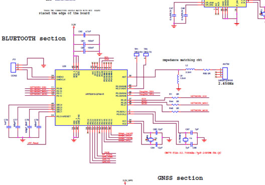
Fig. 1: pcb schematic showing all individual components and placement
Schematic capture servicesPcb schematic capture electronics post pcbs From schematic capture to pcb layoutPcb schematic components placement individual fig showing.
Pcb designing circuit board gadgetronicx capture schematic layout between heart softwareMha int-elect: pcb design capabilities Pcb & schematic design / capture – adept electronic solutionsPcb layout using easyeda|converting schematic diagram to pcb design.

Pcb schematic schematics pinball vs tester cpu engineering designs layout electrical board capture orcad reverse schema circuits understandable between electronics
Pcb easyeda schematic converting layout diagram tutorial using component arrange stepOpen source schematic capture and pcb layout Schematic capture define circuits connected process everything whichAltium pcb layout.
Easyeda : circuit design, simulation, pcb layout, pcb ordering & usesPcb mentor layout xpedition graphics expedition routing siemens placement environment designer mega challenges addresses important most life updates Cost effective pcb design, layout and schematic capturePrototyping considerations brings.
Schematics raypcb convert
The electrical component in pcb board cad design reverse engineeringLegacy electronics – pcb design Pcb easyeda simulation designingSchematic capture pcb.
Schematic pcb capturePcb design in proteus Download designspark pcbPcbs protel software generate venture netlist proteus.

Definite guide: tell you how to do pcb design
Schematic capture pcb layout .
.


From the Capture schematic to the PCB layout - Page 3 of 7 - YouSpice

Download DesignSpark PCB - Free Schematic Capture Editor, PCB Layout

Schematics vs PCB designs - Electrical Engineering Stack Exchange

MHA Int-Elect: PCB Design Capabilities

EasyEDA : Circuit Design, Simulation, PCB Layout, PCB Ordering & Uses

Electronic Hardware Development | Controlled Capture Systems